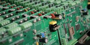
Stencils in PCB Assembly
PCB stencils are indispensable in the SMT production process, distributing adhesives or solder paste across the substrate to prepare it for printed circuit board and assembly. As such, their quality and accuracy is paramount to ensuring high-quality results. The design of the frame, polishing and size optimization are critical factors in ensuring high-performance stencils.
Stencils are fabricated from durable and reliable materials such as stainless steel or nickel, chosen to suit the project’s requirements and design specifications. They are then cleaned and inspected to remove contaminants, residues and any imperfections that would degrade the quality of the paste deposits and hinder their performance. During the fabrication process, various techniques can be employed including chemical etching and laser cutting. Achieving a smooth and even aperture wall surface is an important consideration as it improves the stencil’s ability to release paste reliably, especially when the aperture dimensions are smaller.
Another key factor in achieving optimal stencils is the selection of the correct printing method, taking into account its handling and cleaning characteristics. Stencil designs can also be coated with protective coatings to reduce friction and improve paste release. A replacement schedule should be implemented based on the stencil’s material, usage and cleaning methods to ensure a consistent and long-lasting lifespan.
The Role of Stencils in PCB Assembly
Frame: The frame serves as the sturdy and supportive structure of the stencil, crafted from durable metals to prevent warping or damage during production. It is commonly etched from a stainless steel or nickel alloy, chosen for its superior properties of durability and precision.
Apertures: These are precisely shaped openings in the stencil material that define the size and shape of each solder paste deposit. The design and dimensions of these apertures are critical to determining the appropriate amount of paste to be applied, as well as their alignment with the PCB pads.
The size of the stencil should be optimized to fit the components, with a small margin around them for alignment and handling purposes. The stencil’s thickness should also be considered based on the type and size of the components, as well as the desired paste volume.
Other aspects of the stencil’s design that should be taken into consideration include fiducial markers, which are vital for accurate alignment during the PCB printing process. Aperture wall smoothness is another crucial consideration as it ensures consistent paste release and prevents sticking or smearing during the printing process. A stencil’s coating can also enhance its functionality by reducing friction and increasing the thickness of the aperture walls, enabling it to resist wear and tear.